
Suzhou Hanguang Precision Equipment Co.
Search


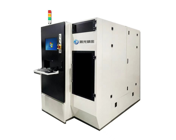
Solution

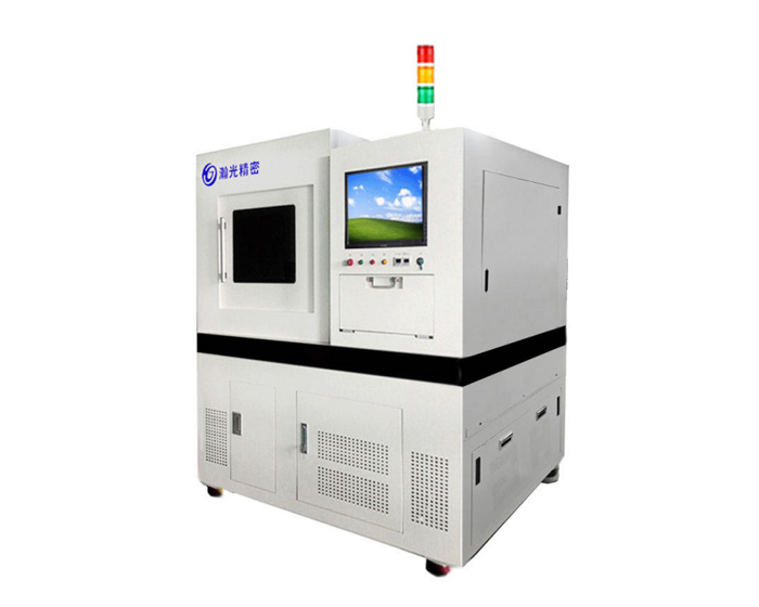
Laser film removal system
Replacing the traditional film removal process for coated glass, we have realised a film removal equipment that can avoid environmental pollution, save consumables, and produce film in a simple, fast and automated way.

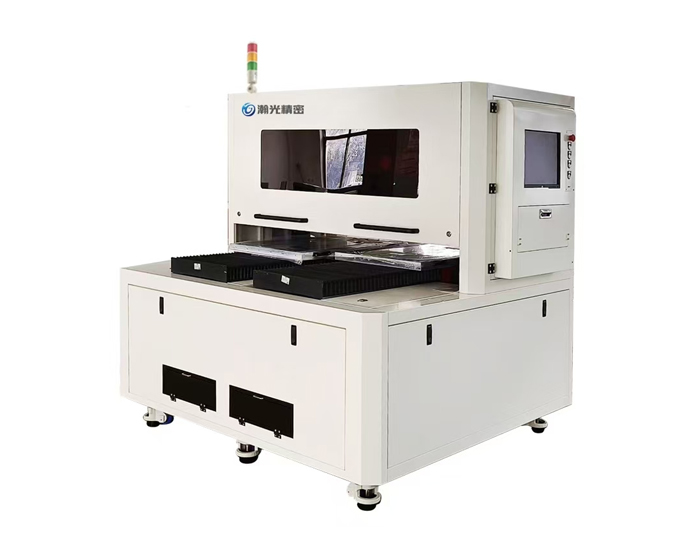
Laser Cutting
Processed with a Bessel focusing head, the high peak power and high peak power density of the Bessel beam is focused inside the glass, instantly vaporising the material in the area to produce a vaporised zone, which rapidly spreads to the upper and lower surfaces to form a crack. The cutting cross-section consists of a myriad of apertures, which are cut by external stress fracture.

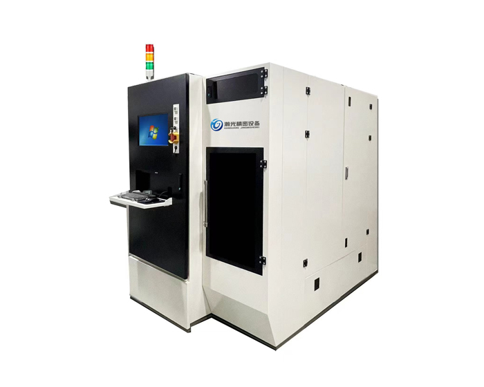
Semiconductor Precision Cutting
Laser technology has penetrated the semiconductor industry and laser processing equipment has been successfully used in the semiconductor field. Highly integrated and high-performance semiconductor wafer demand continues to grow, silicon, silicon carbide, sapphire, glass and indium phosphide and other materials as substrate materials are widely used in the field of semiconductor wafers, laser in the semiconductor industry, glass, sapphire, ceramics and other brittle materials such as precision drilling and cutting, wafer scribing and cutting, etc., has achieved good results in the application of results.

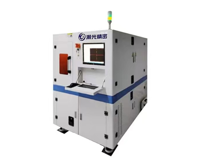
3C Electronics Industry
With the advancement of science and technology, the popularity of the Internet and the improvement of people's living standards, a wealth of consumer electronic products, such as mobile phones, TVs, MP3s, computers, tablets, cameras, wearable smart devices and so on, are changing people's lives in a subtle way.
Products


Scale of Production Capacity
1000+ units/year
Scale of Production Capacity

Technical Accumulation
15年
Technical Accumulation

Patent Certificate
24+
Patent Certificate

Number of Employees
33+
Number of Employees

Production Base
1000+㎡
Production Base

Bachelor's Degree
90%
Bachelor's Degree

Factory Building
1852+㎡
Factory Building

On-site Service
1V1
On-site Service

Team Building
10+
Team Building
News
Company News
Industry News
Latest News


Are you looking for personalised technical support?
Customer-focused, create value for customers, 24-hour response
Enquire Now
Products
Solution
Join Us
About Us
Contact Us
189-1264-3528
E-mail:Luwei@hangglaser.com
Add:1/F, Building 5, No. 45 Dongfu Road, Suzhou Industrial Park, Jiangsu Province, China

All rights reserved:© 2023 Suzhou Hanguang Precision Equipment Co.
File number:Su ICP Bei 2021054439号-1
Technical Support: lit. Shangyun Networks
✕
✕
TOP